8051 Microcontroller Pin Diagram
Pin Diagram Of 8051
8051 Microcontroller Pin Diagram
8051 Microcontroller Pin Diagram
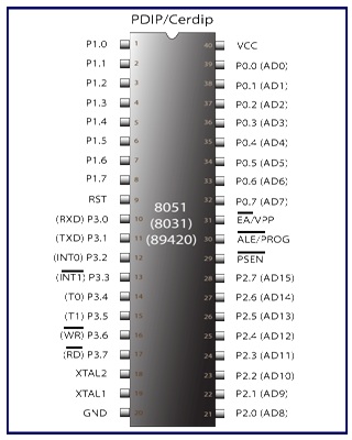
For explaining the pin diagram and pin configuration of microcontroller 8051, we are taking into deliberation a 40 pin Dual inline package (DIP). Now let’s study through pin configuration in brief:-
Pins 1 – 8:- recognized as Port 1. Different from other ports, this port doesn’t provide any other purpose. Port 1 is a domestically pulled up, quasi bi directional Input/output port.
Pin 9:- As made clear previously RESET pin is utilized to set the micro-controller 8051 to its primary values, whereas the micro-controller is functioning or at the early beginning of application. The RESET pin has to be set elevated for two machine rotations.
Pins 10 – 17:- recognized as Port 3. This port also supplies a number of other functions such as timer input, interrupts, serial communication indicators TxD & RxD, control indicators for outside memory interfacing WR & RD, etc. This is a domestic pull up port with quasi bi directional port within.
Pins 18 and 19:- These are employed for interfacing an outer crystal to give system clock.
Pin 20:- Titled as Vss – it symbolizes ground (0 V) association.
Pins- 21-28:- recognized as Port 2 (P 2.0 – P 2.7) – other than serving as Input/output port, senior order address bus indicators are multiplexed with this quasi bi directional port.
Pin- 29:- Program Store Enable or PSEN is employed to interpret sign from outer program memory.
Pin-30:- External Access or EA input is employed to permit or prohibit outer memory interfacing. If there is no outer memory need, this pin is dragged high by linking it to Vcc.
Pin-31:- Aka Address Latch Enable or ALE is brought into play to de-multiplex the address data indication of port 0 (for outer memory interfacing). Two ALE throbs are obtainable for every machine rotation.
Pins 32-39: recognized as Port 0 (P0.0 to P0.7) – other than serving as Input/output port, low order data & address bus signals are multiplexed with this port (to provide the use of outer memory interfacing). This pin is a bi directional Input/output port (the single one in microcontroller 8051) and outer pull up resistors are necessary to utilize this port as Input/output.
Pin-40: termed as Vcc is the chief power supply. By and large it is +5V DC.
related:8051 block diagram explanation, 8051 block diagram explanation pdf, 8051 block diagram pdf, 8051 block diagram ppt, 8051 block diagram download, 8051 block diagram explanation ppt, 8051 microcontroller block diagram explanation, 8051 microcontroller block diagram pdf, 8051 functional block diagram, 8051 internal block diagram, 8051 block diagram, 8051 block diagram and description, 8051 microcontroller block diagram ayala, 8051 architecture block diagram explanation, 8051 architecture block diagram description, 8051 architecture block diagram pdf, atmel 8051 microcontroller block diagram, 8051 controller block diagram, block diagram of 8051 microcontroller, 8051 block diagram description, 8051 microcontroller block diagram description, 8051 microcontroller block diagram with description pdf, digital thermometer using 8051 block diagram, explain 8051 microcontroller block diagram, block diagram for 8051 microcontroller, 8051 microcontroller functional block diagram, 8051 microcontroller functional block diagram pdf, microcontroller 8051 block diagram its description, intel 8051 block diagram, 8051 microcontroller internal block diagram, block diagram of ic 8051, interfacing lcd with 8051 block diagram, block diagram of 8051 trainer kit, 8051 microcontroller block diagram, 8051 microcontroller block diagram ppt, 8051 microprocessor block diagram, 8051 mc block diagram, 8051 microcontroller architecture block diagram, block diagram of 8051 microcontroller description, block diagram of 8051 microcontroller pdf, block diagram of 8051 microcontroller ppt, block diagram of 8051 microprocessor, block diagram of 8051 architecture, block diagram of 8051 mc, block diagram of 8051 pdf, functional block diagram of 8051 microcontroller, 8051 timer block diagram, block diagram of the 8051, 8051 uart block diagram, 8051 microcontroller block diagram with description, block diagram of 8051 with explanation,
related:8051 block diagram explanation, 8051 block diagram explanation pdf, 8051 block diagram pdf, 8051 block diagram ppt, 8051 block diagram download, 8051 block diagram explanation ppt, 8051 microcontroller block diagram explanation, 8051 microcontroller block diagram pdf, 8051 functional block diagram, 8051 internal block diagram, 8051 block diagram, 8051 block diagram and description, 8051 microcontroller block diagram ayala, 8051 architecture block diagram explanation, 8051 architecture block diagram description, 8051 architecture block diagram pdf, atmel 8051 microcontroller block diagram, 8051 controller block diagram, block diagram of 8051 microcontroller, 8051 block diagram description, 8051 microcontroller block diagram description, 8051 microcontroller block diagram with description pdf, digital thermometer using 8051 block diagram, explain 8051 microcontroller block diagram, block diagram for 8051 microcontroller, 8051 microcontroller functional block diagram, 8051 microcontroller functional block diagram pdf, microcontroller 8051 block diagram its description, intel 8051 block diagram, 8051 microcontroller internal block diagram, block diagram of ic 8051, interfacing lcd with 8051 block diagram, block diagram of 8051 trainer kit, 8051 microcontroller block diagram, 8051 microcontroller block diagram ppt, 8051 microprocessor block diagram, 8051 mc block diagram, 8051 microcontroller architecture block diagram, block diagram of 8051 microcontroller description, block diagram of 8051 microcontroller pdf, block diagram of 8051 microcontroller ppt, block diagram of 8051 microprocessor, block diagram of 8051 architecture, block diagram of 8051 mc, block diagram of 8051 pdf, functional block diagram of 8051 microcontroller, 8051 timer block diagram, block diagram of the 8051, 8051 uart block diagram, 8051 microcontroller block diagram with description, block diagram of 8051 with explanation,


0 comments:
Post a Comment
If you have any questions or droughts feel free to ask here.